
Semiconductor buildout shifts toward packaging capacity
Three of the largest announced investments this quarter target advanced packaging rather than fabrication.
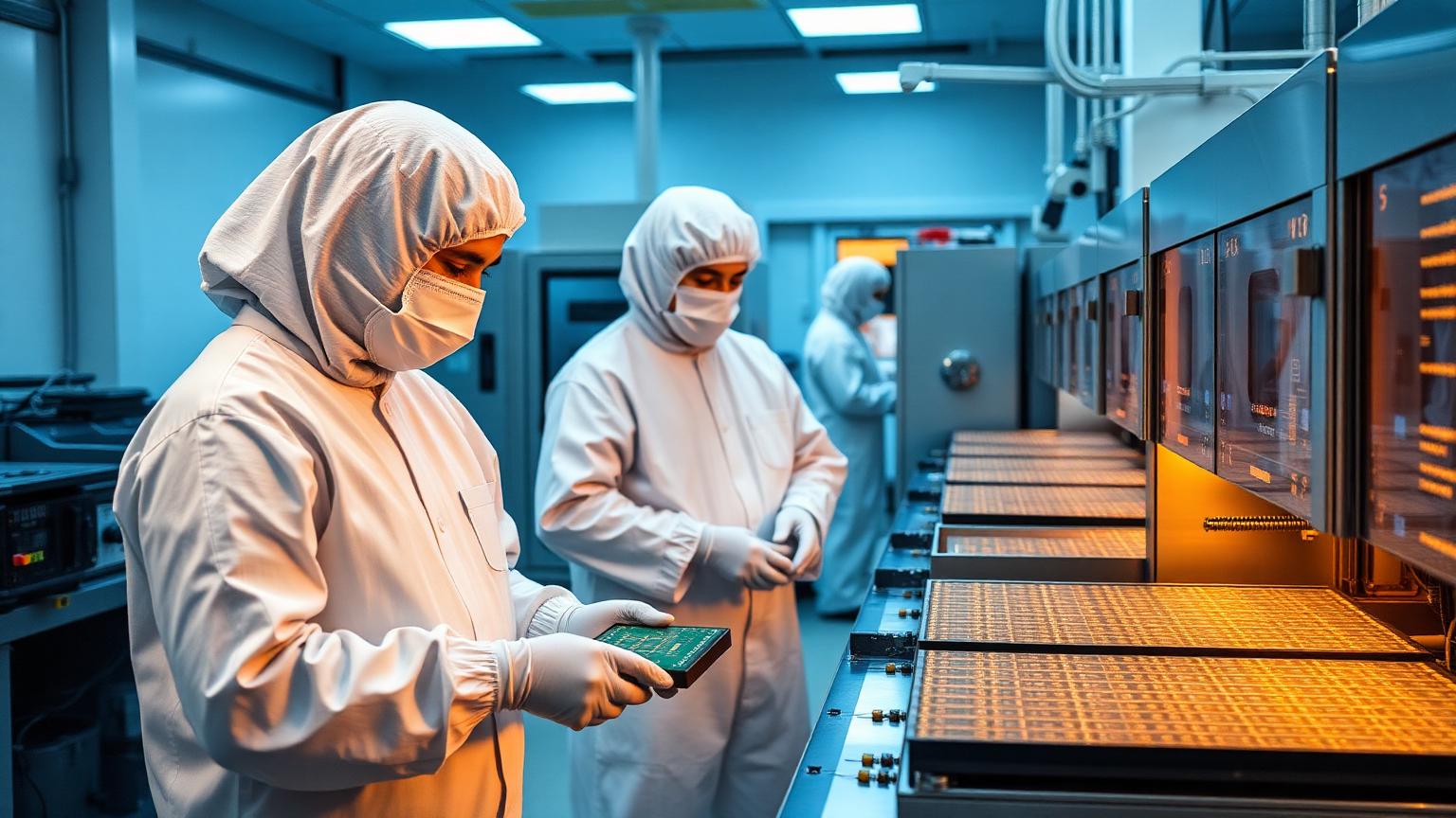
- Three of the quarter's largest investments target advanced packaging.
- Packaging has become the binding constraint for high-bandwidth memory assemblies.
- Lead times for packaging equipment remain above sixty weeks.
Machine-generated from the reporting on this page and reviewed by an AMN editor before publication.
The largest semiconductor investments announced this quarter share a characteristic that would have been unusual three years ago: they are for packaging, not fabrication.
Advanced packaging has become the binding constraint on high-bandwidth memory assemblies, and the industry has responded by committing capital to the step it previously treated as commodity back-end work.
Equipment lead times remain above sixty weeks, which sets a floor on how quickly any of this capacity arrives.
Two of the three announcements involve joint ventures between a foundry and a memory supplier, a structure that barely existed before 2024.
Analysts expect the packaging share of total capital expenditure to keep rising through at least 2028.